|
Characterizations and applications of nanomaterials |
|||||
High-efficiency photo-electron conversion devices Semiconductor processes and nanofabrication Characterizations and applications of nanomaterials Optical characterization of graphene Graphene-gold oxide photodetector Optical analysis of hollow gold nanoparticles Photomodification of hollow gold nanoparticles for high-density data storage Light harvesting and light extraction Light extraction efficiency of LEDs Antireflection structures for solar cells Optical analysis techniques Eco-friendly devices and sensors
|
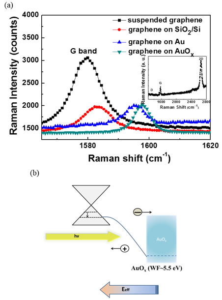
Transparent, broadband, and bifacial-operable flexible photodetectors containing a large-area graphene–gold oxide heterojunction In this study, we combine graphene with gold oxide (AuOx), a transparent and high work-function electrode material, to achieve a high efficient, low-bias, large-area, flexible, transparent, broadband and bifacial-operable photodetector. The photodetector operates through hot electrons being generated in the graphene and charge separation occurring at the AuOx–graphene heterojunction. The large-area graphene covering the AuOx electrode efficiently prevented reduction of its surface; it also acted as a square-centimeter-scale active area for light harvesting and photodetection. Our graphene/AuOx photodetector displays high responsivity under low-intensity light illumination, demonstrating picowatt sensitivity in the ultraviolet (UV) regime and nanowatt sensitivity in the infrared (IR) regime for optical telecommunication. In addition, this photodetector not only exhibited broadband (from UV to IR) high responsivity—3300 A W–1 at 310 nm (UV), 58.2 A W–1 at 500 nm (visible), and 8.85 A W–1 at 1550 nm (IR)—but also required only a low applied bias (0.1 V). The hot-carrier-assisted photoresponse was excellent, especially in the short-wavelength regime. In addition, the graphene/AuOx photodetector exhibited great flexibility and stability. Moreover, such vertical heterojunction–based graphene/AuOx photodetectors should be compatible with other transparent optoelectronic devices, suggesting applications in flexible and wearable optoelectronic technologies. KEYWORDS: gold oxide (AuOx), graphene, transparent, photodetector, heterojunction, flexible device, bifacial operation |
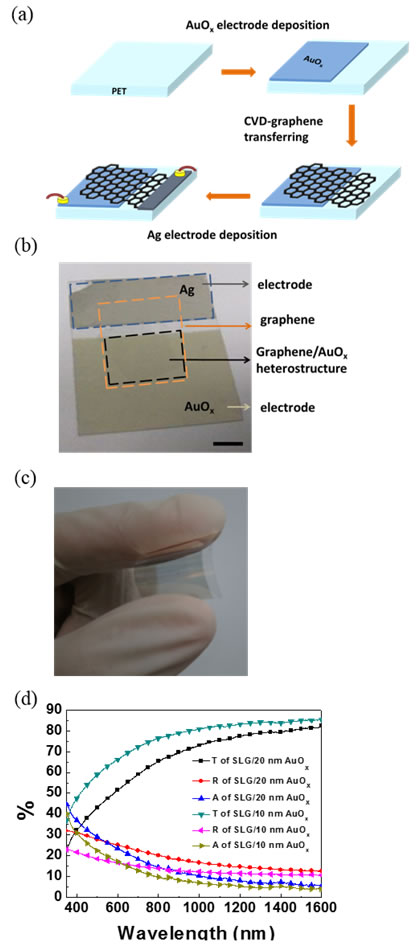
(a) Schematic representation of the fabrication of a graphene/AuOx vertical heterostructure on a PET substrate. (b) Photograph of the graphene/AuOx photodetector; scale bar: 10 mm. (c) Photograph revealing the flexibility and transparency of the graphene/AuOx photodetector. (d) Transmittance, reflectance, and absorbance spectra of graphene/AuOx systems having various thicknesses of the AuOx layer on PET substrates.
|
|||
Copyright(c) 2008 Nano-optpelectronics Lab., Department of Material Science and Engineering, National Taiwan University No. 1, Sec. 4, Roosevelt Road, Taipei, 10617 Taiwan(R.O.C) Phone:+886-2-3366-3240 Fax:+886-2-2362-7651 |
|||||